![]()
INTRODUCTION
A charge coupled device (CCD) is a detector that provides digital images, unlike conventional film. The digital format allows the images to be manipulated by a computer, which can electronically sharpen, modify, or copy them.
CCDs are used to take photographs of very faint and distant stars. They are used to make accurate measurements of position, and therefore of speed and acceleration. They also serve as detectors in x-ray diffraction experiments. In each case the large detection area allows a great deal of information to be collected simultaneously.
|
(picture of a commercially available digital camera) Picture courtesy of Sony Corporation |
In movie-making, CCD cameras are useful for adding special effects. Previously, the scene was shot on conventional film and then scanned into a computer. This process was slow, and image quality was lost in the process. With a CCD, the scene is placed directly onto a computer for editing. A CCD relies on semiconductor properties for its operation. Basically, photons of certain energies strike a layer of silicon, promoting electrons into the conduction band. A CCD collects and counts these electrons to determine how many photons were absorbed by the silicon. |
BASIC DESIGN
Every CCD starts with a backing of some sort, usually glass. The backing is then covered with metal electrodes, as shown in Figure 1 below. The bottom row of electrodes is designated as the readout register.
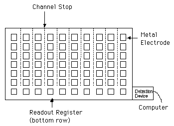
Figure 1
A thin layer of silicon dioxide is placed on top of the electrodes. Above the silicon dioxide is a layer of n-type silicon. Finally, a thin layer of p-type silicon lies atop the n-type silicon. This creates a p-n junction that covers the electrodes. The purpose of the silicon dioxide is to separate electrically the silicon from the electrodes. This helps to isolate the electrons in the silicon.
Between each column of electrodes there is a channel stop, indicated by dashed lines in Figure 1. Channel stops prevent electrons from flowing horizontally across the CCD array. There are no channel stops in the readout register; in this row, charges are free to move horizontally to the detection device. A side view of a CCD is shown in Figure 2.
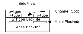
Figure 2
HOW DO THEY WORK?
Each CCD is divided into many groups of electrodes called pixels. The exact number of pixels depends on the individual pixel size and the cost of the array. Typically, a low-cost commercial array has dimensions of 600 x 300 pixels, while high cost arrays for scientific applications have dimensions closer to 3000 x 3000 pixels. Each pixel has two, three, or four electrodes in it with three being the most common.
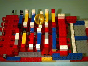
Figure 3 shows a LEGO model of a CCD. The three vertical black tracks represent rows of electrodes. The vertical red bars represent the channel stops while the gray bricks denote boundaries between pixels. The horizontal black track along the bottom represents the readout register. The light/light sensor array in the lower left acts as the detection device for the LEGO model.
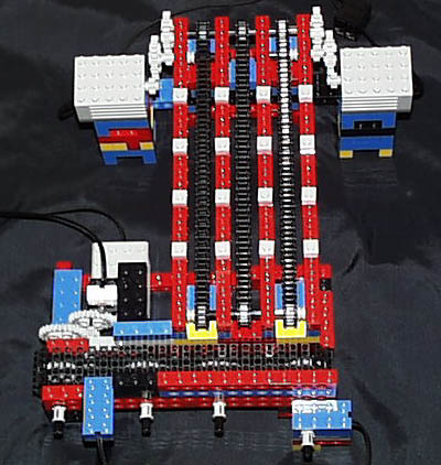
Figure 3
As photons of light enter the CCD, they are absorbed by the silicon layer if they have sufficient energy. Each absorbed photon causes an electron to be promoted into the conduction band. During CCD photography, for every one hundred incident photons, between forty and eighty are absorbed by the silicon. (Conventional photographic film absorbs approximately 2% of all incident photons.) The electrons then collect above the center electrode, which has been positively charged. In theory, one could construct a CCD that collects the holes instead of the electrons. In practice, however, it is easier to count electrons.
Band Gap Animation
Note: The arrow keys may be used to step through all animations one frame at a time.
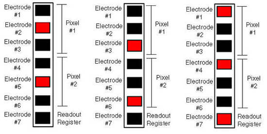
After the exposure is completed, all of the collected electrons are sequentially moved to the detection device where they are counted. This is accomplished by changing the charge on the electrodes in a timed, sequential manner.
|
Figure 4a |
Figure 4b |
Figure 4c |
To illustrate, electrodes 2 and 5 are initially positively charged and so collect all the electrons photogenerated around them, Figure 4a. Next, electrodes 3 and 6 gradually begin to acquire positive charge while 2 and 5 gradually become negatively charged. This causes the electrons to move to electrodes 3 and 6, Figure 4b. Then, electrodes 1, 4, and 7 gain positive charge while 3 and 6 become negatively charged. This causes the electrons to move once more, Figure 4c. The electrons from the bottom most-pixel (pixel #2) are now in the readout register, electrode 7.
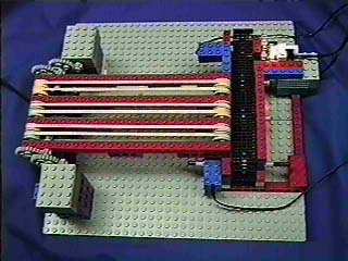
The LEGOs motors in Figure 3 serve an analogous purpose. They move the bricks, representing electrons,to the detection device while the rotation sensor, shown on the lower right, keeps track of where each brick came from. Shown in Figure 5 is a LEGO model better suited to demonstrate electron motion.
|
|
|
|
Figure 5a |
Figure 5b |
Here the ball represents an electron and each bar represents an electrode. Height is inversely proportional to charge in this model, the lower the bar the more positively charged the electrode. As each electrode is sequentially lowered, gravity causes the ball moves to the right.
The readout register now begins to deliver the electrons to the detection device by the same process of varying the voltage applied to the electrodes, but now across the bottom row. The detection device counts the number of electrons by applying a known voltage across the final electrode. (The final electrode is located inside the detection device, not on the CCD array.) The voltage will increase slightly as it picks up electrons from the CCD. By subtracting the background voltage, the voltage from the CCD electrons can be found. The number of electrons can then be calculated using Faraday's constant and this voltage increase.
Electrons from pixel #1 would follow the same procedure. They would be the next group to be moved into the readout register and to the detection device.
Finally a computer takes the numbers from the detection device and uses them as relative intensities to display the image on the screen. It takes as little as 100 ms to completely move all electrons from a 2000 x 2000 pixel CCD to the detection device. Exposure time may be much longer for low level light sources.
|
|
|
|
Note: Colors in this animation represent electric fields. |
|
|
The metal electrodes are not actually in electrical contact. |
Side View CCD Animation
HOW COLOR IS ADDED
The CCD previously described is strictly gray-scale. Although blue photons have more energy than red photons, each photon promotes only one electron. Once an electron is promoted into the conduction band, which requires a minimum amount of energy called band gap energy, any extra energy the electron has is bled off in the form of vibrations of atoms in the solid until the electron is at the bottom of the conduction band. Thus, a CCD cannot differentiate between a red or a blue photon because only numbers of electrons are counted. In order to provide color images, a number of gray-scale pixels are covered with colored filters and combined to make a single color pixel. Each gray-scale pixel is electronically swept out in the same way as before. The computer then takes the data from each gray-scale pixel and uses it as the red, green, and blue components of the color pixel.
Color Band Gap Animation
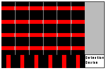
One would imagine that equal numbers of each of the primary colors, red, green, and blue, would allow a CCD to obtain a correct color image, but in fact this is not true. Color CCDs generally have 50% to 75% green pixels. The human eye is more sensitive to green light so in order to make the images "look right", the CCD must also have extra sensitivity to green light. A typical arrangement of colored pixels is shown in Figure 6.
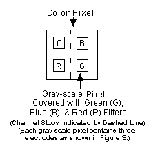
Figure 6
LIMITATIONS
CCDs are very expensive and complex instruments. A low-cost astronomical imager costs around $2000 while top-of-the-line imagers cost more than $50,000. In order to take a quality picture, the CCD must be calibrated. Differences in pixel sensitivity must be taken into account, dark current must be reduced, and transfer rates must be synchronized.
Pixel sensitivity is the ratio of collected electrons to incident photons and this quantity varies from pixel to pixel. It is fairly easy to calibrate a CCD array to minimize variations in pixel sensitivity. Ideally, if the CCD were uniformly illuminated then pixel sensitivity could be mapped and mathematically compensated for by a computer. Uniform illumination is accomplished by taking pictures of a perfectly white spot.
Thermal energy causes electrons to be promoted to the conduction band. These electrons are then counted as photons even though they were not created by photons. This is called dark current. If the temperature of the CCD were reduced, dark current would also be reduced. In commercial applications, dark current is not a significant factor, but in higher grade scientific CCDs, a liquid nitrogen cooling system is used to reduce dark current. The general rule of thumb is dark current is cut in half for every seven or eight degrees Celsius drop in temperature.
To attain optimum image quality, all electrons from any given row must be transferred into the readout register at precisely the same time. This requires the electrodes to change their charge at the same time and at the same rate. The procedure for ensuring that all transfer rates are perfectly synchronized is very complex. The manufacturer usually synchronizes the transfer rates before sending out a CCD.
APPLICATIONS
There are many different types of CCDs. The one previously described was just one example of how CCDs are constructed. There are three main types of CCDs, each with strengths and weaknesses.
|
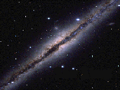
Picture Courtesy of the University of Wisconsin Astronomy Department |
Full frame CCD is the exact name of the array described above. These are commonly used in astronomy because they are capable of long exposure times. The photograph shown on the left was taken with a CCD camera. This is a picture of spiral galaxy NGC 891. |
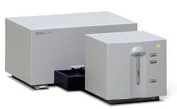
| Linear array CCDs are simplified full frame CCDs. They have only one row of pixels with a detection device on the end. This type of CCD is commonly used in chemistry as a detector for high performance liquid chromatography and for certain spectrophotometers. The picture on the right is a spectrophotometer which uses a charge coupled device as a detector. Shown on the right is an HP 8453 diode-array spectrophotometer. |
Picture Courtesy of Hewlett Packard |
|
Picture Courtesy of KeySonic Technology Inc. |
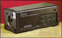
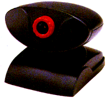
Interline transfer CCDs have readout registers intermingled with the electrodes in the array itself (see Figure 7 below). Instead of traveling down the array to reach the readout register, electrons are moved one column to the right, into a shielded readout register, and then down. This reduces readout time to a minimum and allows the highest number of pictures per minute. Only half of each array is sensitive to light, however, so some image quality is lost. This type of CCD is highly advantageous in movie cameras, where frame rate is the main issue and display screens are the limiting factor controlling image quality. Physicists measuring speed and acceleration also find interline transfer CCDs useful. The high frame rate allows them to make very accurate measurements of position, and therefore of speed and acceleration. The picture on the left is of a USB CCD Video Camera. The interline transfer CCD inside contains 250,000 pixels arranged in 525 lines. |
![]()
Figure 7
Progressive scan is not really a type of CCD. It is more properly a technique for using a full frame CCD. Progressive scan permits long exposure times of moving objects and is a useful quality control mechanism in manufacturing plants. As an object moves down the assembly line, a CCD takes its picture and relays that to a computer, which then determines whether the object has been correctly manufactured or not. As the object moves, the electrons forming the image are moved across the CCD at the same rate, or a lens is used to adjust the rate. Thus, even though the object is moving, all photons from the object combine on the CCD array. This technique is not more widely used because the exact speed of the object must be a known constant. Differences in pixel sensitivity and dark current have a multiplied effect, reducing image quality.
FUNDAMENTAL DIFFERENCES IN CONSTRUCTION
A four-phase CCD is an array with four electrodes per pixel instead of the three previously described. In a four phase CCD, the electrodes work in pairs. Electrons are always shared between two adjacent electrodes. Because there are so many electrodes per pixel, only 25% of the total area is available for data collection. This leads to very low resolution. Four phase CCDs were originally designed because the timing required to move electrons from electrode to electrode was fairly easy to achieve.
In order to produce a CCD with only two electrodes per pixel, the construction of the silicon layer must be altered. To keep the electrons moving toward the readout array and not sliding backwards, the silicon dioxide layer is sloped so that it is thinner near the readout array and thicker at the top. The electrons, which want to get as close to the positively charged electrodes as possible, naturally migrate down this electron slide.
Side View of a 2 Phase CCD
CONCLUSION
Charge coupled devices rely on the chemical properties of semiconductors for their operation. Photons of certain energies strike a layer of silicon freeing an electron from the lattice. The CCD then collects and counts these free electrons.
CCDs are being used in a wide variety of places for a wide variety of purposes. They are being used as high precision scientific instruments as well as low cost commercial products. This versatility accounts for the speed at which charge coupled devices are being adopted in the marketplace.
Copyright 2001 by the University of Wisconsin - Madison Materials Research Science and Engineering Center for Nanostructured Materials and Interfaces, Board of Trustees of Bradley University. All rights reserved. This project was supported, in part, by the National Science Foundation. Opinions expressed are those of the authors and not necessarily those of the Foundation. LEGO and DACTA are trademarks of the LEGO group and are used with special permission. © 2001 the LEGO group. The illustrations in these experiments are used here with special permission.