
![]()
The number of electrons generated by dark current is given by the equation
![]()
where ![]() is the dark current density,
is the dark current density, ![]() is the area
of the detector,
is the area
of the detector, ![]() is the time the array is exposed to light, and
q is the charge on one electron. Dark current density,
is the time the array is exposed to light, and
q is the charge on one electron. Dark current density, ![]() , is given by the equation
, is given by the equation
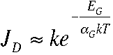
where![]() is the band gap energy, 1<
is the band gap energy, 1<![]() < 2, and
kT is thermal energy.
< 2, and
kT is thermal energy.
Individual pixel sizes range from 20 um x 20 um to 5 um x 5 um. The total size of the array affects these numbers somewhat, but mostly they depend on the manufacturer.
Image quality depends on both individual pixel size and the number of pixels per array. Smaller pixels can be placed closer together. This increases the number of pixels per square centimeter, thus increasing resolution and image quality. More pixels per array increases the area of the detector. This allows the image to be enlarged using a transparent lens, assuming the same field of view is desired. A larger image also increases the number of pixels used to collect data about the image, increasing resolution and image quality.
Not every photon that strikes the surface of a CCD promotes an electron into the conduction band to be counted. Some photons have such a long penetration depth that they go right through the silicon without being absorbed. Others are absorbed at the surface where the electrons recombine with the holes right away. Some CCDs have extra layers designed to adjust the penetration depth in order to be sensitive to different photon wavelengths.
Due to imperfect manufacturing techniques, certain areas of the silicon layer are more sensitive to photons than others. Thus the electrodes underneath these areas consistently register more electrons than others, even under uniform lighting.
A p-n junction is prepared by a process called doping. Doping is the deliberate substitution of impurity atoms into a host crystal, in this case silicon. p-Type silicon is pure silicon that has been doped with atoms having fewer valence electrons than silicon, such as gallium. Since these dopant atoms have fewer valence electrons, so-called "holes" are created in the silicon lattice. In contrast, n-type silicon is doped with elements having more valence electrons than silicon, such as phosphorus. These extra electrons are not involved in bonding and are free to move around the solid. A p-n junction occurs where n-type and p-type materials come in contact with each other. The extra electrons from the n-type silicon move to fill the holes in the p-type silicon. This leaves a net positive charge in the n-type silicon because electrons have left, and a net negative charge in the p-type side. The electric field created by these net charges aids in collection of the photogenerated electrons.
The equation used to calculate the number of electrons on the final electrode is
![]()
where G is the gain of the detector itself, q is the electronic charge, ![]() is the number of electrons, and C is a constant specific
to each CCD.
is the number of electrons, and C is a constant specific
to each CCD.
Copyright 2001 by the University of Wisconsin - Madison Materials Research Science and Engineering Center for Nanostructured Materials and Interfaces, Board of Trustees of Bradley University. All rights reserved. This project was supported, in part, by the National Science Foundation. Opinions expressed are those of the authors and not necessarily those of the Foundation. LEGO and DACTA are trademarks of the LEGO group and are used with special permission. © 2001 the LEGO group. The illustrations in these experiments are used here with special permission.