
Individual Atom Manipulation
Introduction
If you wanted to build a fort out of pillows you would go around the house and collect several cushions then simply arrange them with your hands. What if you wanted to build a fort out atoms? How could you build a structure out of something you can't pick up, let alone see?
When scientists want to build something on the nanoscale they have two choices:
(1) they can have the different building blocks come together on their own (also known as self-assembly),
(2) they can move the different building blocks individually.
The smallest building block out there is the atom. Within the last 20 years scientists have learned how to move atoms individually - an amazing feat because atoms are extraordinarily small. This process is called atom manipulation.
The Invention of the STM
Before scientists could build at the atomic scale they needed a tool to help them observe it. Before the 1980's there was no instrument or microscope that could image the atomic scale.
In 1981 the Scanning Tunneling Microscope (STM) was invented by Gerd Binning and Heinrich Rohrer at IBM; the pair later received the 1986 Nobel Prize in physics for this accomplishment. The STM has ultra-high resolution and can image single atoms. This instrument allowed scientists to view a world that they could not view before: the world of the nanoscale. Many people believe that the invention of the STM was the birth of nanoscience.
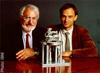
Binning and Rohrer with their Nobel prize1
"Seeing" an atom
No one has ever seen an atom. The wavelength of visible light is more than 1000 times bigger than an atom, so light can not be used to see an atom.
Scanning Tunneling Microscopes work by moving a probe tip over a surface we want to image. The probe tip is an extremely sharp - just one or two atoms at its point. There is a small electric voltage on the probe tip and depending on the height of different parts of the surface, more or less current will flow from the tip to the surface. By noting the changes in current we can recreate an image of the surface at the atomic level.
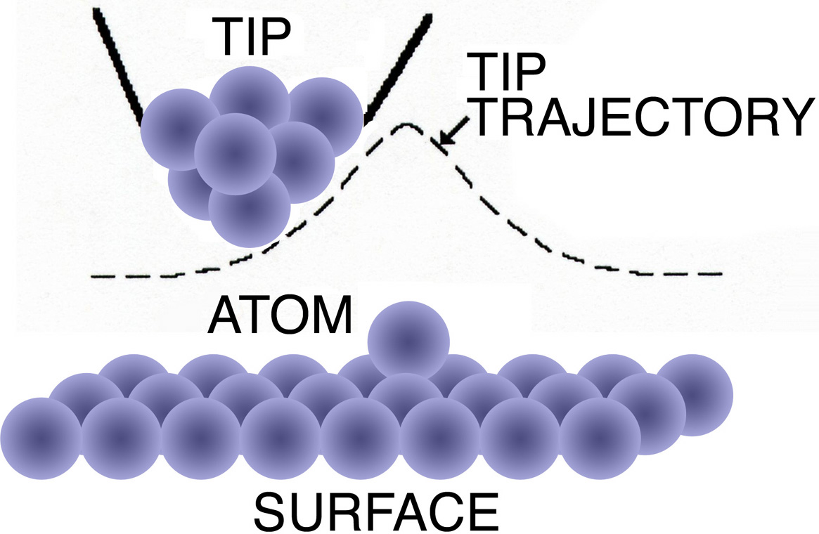
As the tip moves over a surface, it "feels" atoms as increases in current.
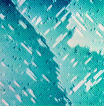
An STM image of a silicon surface - each bump is one atom.
Atom Manipulation
STM can be used not only to image atoms but to move them as well. This was first shown by Don Eigler in 1989 when he released this image of 35 Xenon atoms arranged on a surface. Can you guess what company he worked for?
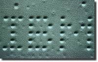
Xenon atoms on a nickel surface.2
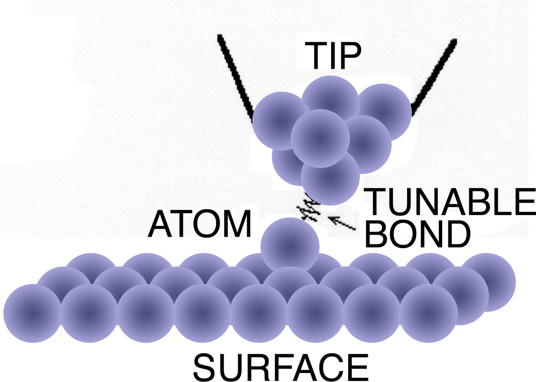
Increasing the current creates a bond between the tip and the atom.
References
1. Image from IBM