
Probe Microscopes
Could you pick up a boulder with a pair of tweezers? Could you pick up a piece of hair with a bulldozer? Having the right size tools for the job can be pretty important. When scientists study the nanoscale, they need to use tools that are the right size. To study things that are very, very small, they need very, very small tools.
Introduction
Scanning probe microscopes are a set of tools with very small parts that help scientists image the nanoscale. Each type of scanning probe microscope involves a very fine probe tip that scans back and forth over a surface. The ability to image individual atoms in scanning probe microscopies can be mimicked with a refrigerator magnet.
The first SPM was the scanning tunneling microscope (STM). STM is limited to surfaces that are electrically conductive. Later, Atomic Force Microscopy (AFM) was invented, which could scan any surface, conductive or not.
Before STM was invented, scientists and engineers could not "see" atoms or atomic scale features. The technique was invented in 1981 by a couple of IBM researchers, Gerd Binnig and Heinrich Rohrer, at the Rueschlikon, Switzerland IBM facility. With the discovery of this technique, scientists could look at the atomic level upward. It came just in time for the semiconductor industry that needed to locate and measure the size and performance of chips.
In 1982 Binnig and Rohrer reported using a STM to see atoms in a silicon sample. For the development of the STM, they won the Nobel Prize in physics in 1986. Binnig, Christoph Gerber (IBM Zurich), and C. F. Quate (Stanford University) are credited with the development of the atomic force microscope (AFM). In 1987 Tom Alrecht was the first to see atoms using a AFM. In 2007 the first cases of identification of atoms in the surface of a material were reported using a AFM. Each element in the alloy was first investigated to determine the amount of interaction there was with the probe. Then atoms of those elements were identified in the surface by "feeling" the atoms with the probe and identifiying the element based on the amount of interaction.
Some of the other forms of scanning probe microscopy include: Magnetic Force Microscopy, MFM; Chemical Force Microscopy, CFM; Scanning Force Micrsocopy, SFM; and Electrostatic or Electric Force Micrsocopy, EFM.
How they work
Scanning Tunneling Microscopes (STMs)
Scanning Tunneling Microscopes work by moving a probe tip over a surface we want to image. The probe tip is an extremely sharp - just one or two atoms at its point.
Scanning Tunneling Microscopy operates in either of two methods. One method allows the probe to approach the surface until a specific flow of current is achieved. The probe this repsonds up or down to maintain that value of current. The second method maintains a specific height above the surface with the probe and the amount of current flow is measured. By noting the changes in current we can recreate an image of the surface at the atomic level.
 |
| As the tip moves over a surface, it "feels" atoms as increases in current. |
In both cases the probe needs to be near atomically sharp.
 |
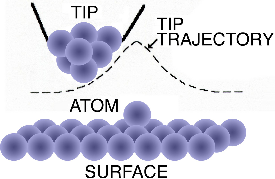
| In this image we see a surface with a single atom on that surface and a collection of 6 more atoms on the surface. The "dull" probe in this view will not be able to characterize this surface very well as the features of the probe are larger that some of the features in the surface. |
For the probe to be effective in characterizing the surface, its features must be smaller than those of the surface being characterized.
 |
With the sharper tip, the surface can be better characterized as the tip can drop down in the area between the single atom and the layer of 6 atoms. View a video of this. |
In the figure below we see the basic components of scanning probe microscopy: the probe tip attached to a cantilever, a laser, and a detector.
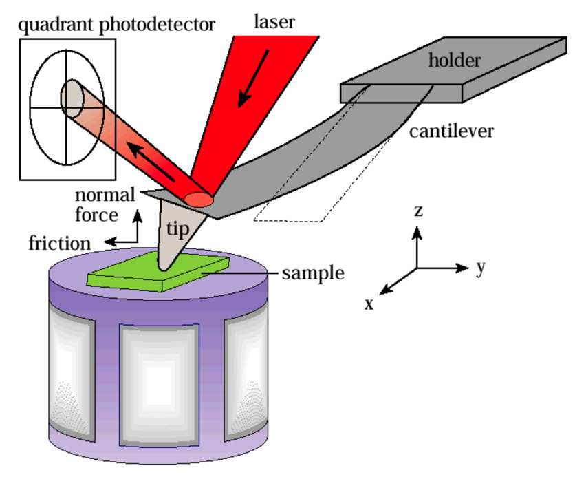 |
| An "atomically sharp" tip raster-scans over the surface. A laser is reflected off the back of the probe to the detector. Very small movements in the tip are amplified onto the detector. |
Atomic Force Microscopes (AFMs)
AFMs can be used in air, in liquids, in gases, and under high vacuum and are being used throughout the scientific community. AFMs are member of the scanned-proximity probe microscopes, meaning the the probe does not come into contact with the sample, it just gets close enough to the surface to sense the forces of the sample. There is an attractive force between the tip and the surface and this force is kept the same throughout the experiment. As the probe tip scans back and forth over the surface, the tip will rise and fall with the different features on the surface.
Since all this is going on at a very small scale, we can't watch the tip directly. A laser is pointed at the tip and is reflected to a sensor. As the tip goes up and down the laser hits different parts of the sensor. With the information the sensor collects, an image of the surface can be recreated.Raster-scans of the surface create an image much like a television, one line after another. In this way, AFMs can be used to determine the topography of the surface, as well as optical and magentic properties of the surface.
Applications
Imaging with Probe Microscopes
No one has ever seen an atom. The wavelength of visible light is more than 1000 times bigger than an atom, so light can not be used to see an atom. However, probe microscopes can recreate images of atomic surfaces.
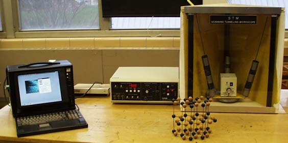
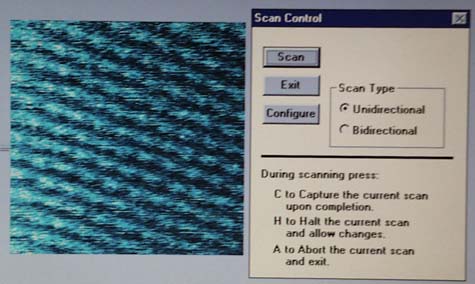
Here we see a student grade portable Scanning Tunneling Microscope and an image of the surface of graphite taken at the Engineering Expo in April, 1999:
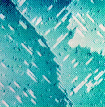
The surface of Silicon was imaged by Prof. Max Lagally, University of Wisconsin - Madison. Note the various layers of atoms.The lighter colored rows represent layers on top of the bottom most layer. Also note the dark spots that represent holes in the layers where silcon atoms are missing.
Don Igler and group and IBM used an AFM to create their now famous "Quantum Corral" by arranging iron atoms in a circle on a copper subtract. The atoms were arranged using the probe from the AFM to move the atoms across the surface. With the iron atoms in a perfect circle, the electrons in the copper surface set up a standing wave.
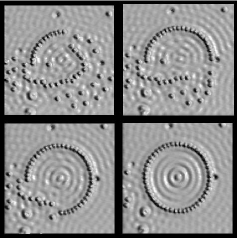 |
Don Eigler arranged 48 iron atoms on the surface of a copper substrate. These images show the various stages of the process. Once complete the circular arrangement of the iron atoms forced the electrons in the surface of the copper to specific quantum states as shown by the rippled appearance of the surface. |
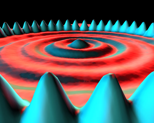 |
"Quantum corral" of iron atoms on the surface of a copper substrate created the wave effect with the electrons in the copper atoms on the surface. |
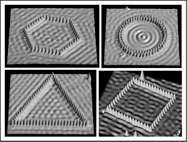 |
| Other arrangments of iron atoms on copper substrates. Note that only the perfect circle shows the standing wave of electrons. |
Individual Atom Manipulation
If you wanted to build a fort out of pillows you would go around the house and collect several cushions then simply arrange them with your hands. What if you wanted to build a fort out atoms? How could you build a structure out of something you can't pick up, let alone see?
When scientists want to build something on the nanoscale they have two choices:
- they can have the different building blocks come together on their own (also known as self-assembly),
- they can move the different building blocks individually.
The smallest building block out there is the atom. Within the last 20 years scientists have learned how to move atoms individually - an amazing feat because atoms are extraordinarily small. This process is called atom manipulation.
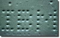
STM can be used not only to image atoms but to move them as well. This was first shown by Don Eigler in 1989 when he released this image of 35 Xenon atoms arranged on a surface. Can you guess what company he worked for?
 |
|
Xenon atoms on a nickel surface. (2) |
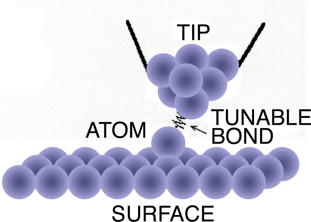
Atoms can be moved on surfaces with STM by creating a what is called a tunable bond between the probe tip and the atom. When the current flowing between the atom and the probe tip increases, the atom gets stuck under the tip. The tip with the atom can then be moved to another part of the surface and the current decreased to let the atom go from the tip.
 |
|
Increasing the current creates a bond between the tip and the atom. |