

LEDs - Light Emitting
Diodes
Band Theory
As described below, simple chemical bonding ideas can be used to provide a qualitative
understanding of how the color of light emitted by an LED is tuned by changes
in the semiconductor's chemical composition.
The following is a brief review of the band theory under pinning these devices.
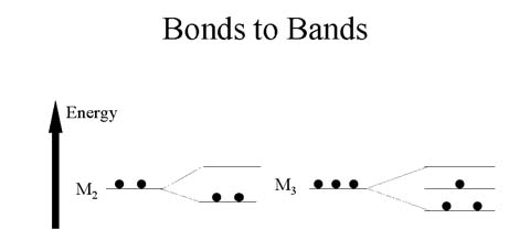
When two atoms bond together to form M2, two molecular orbitals are
formed. When three atoms bond together to form M3, three molecular
orbitals are formed.
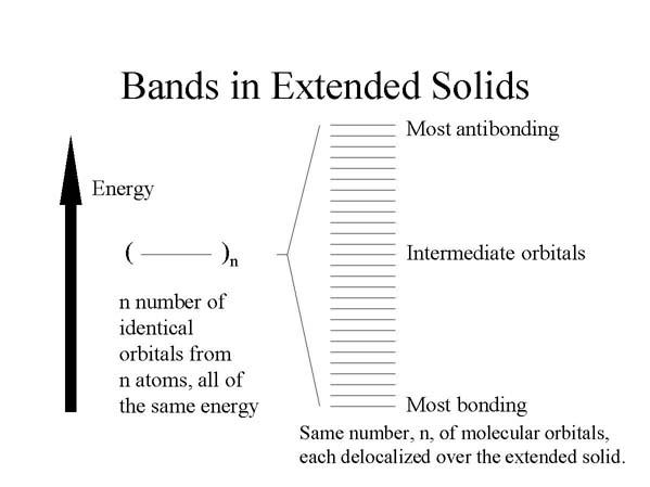
In the extended solid, many atoms interact with one another, and there will be
the same number of molecular orbitals, delocalized over the entire solid, as
the number of atomic orbitals being combined. The energy separation of the orbitals
is so small from one such delocalized orbital to the next that they comprise
a so-called "band." The band represents a kind of electronic highway allowing
electrons to move throughout the solid, thereby conducting electricity. For this
to occur, however, the band cannot be empty or filled with electrons. Only if
the band is partially filled can a net flow of electrons occur, corresponding
to an electrical current.
The band containing the valence electrons is known as the valence band. The band of unoccupied orbitals is known as the conduction band. Conduction occurs
when electrons are promoted from the valence band to the conduction band, where
they can move throughout the solid. The energy separation between the valence
and conduction bands is known as the bandgap energy.
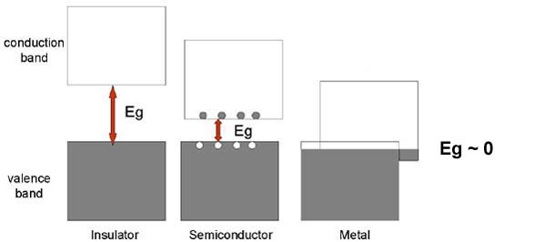
Schematic band diagrams for an insulator, a semiconductor, and a metal.
The band gap energy, Eg, shown as the double-headed arrow, is the separation
between the top of the valence band and the bottom of the conduction band. The
size of the band gap decreases in passing from aninsulator to a semiconductor
to a metal, where it is effectively zero. Electron-hole pairs are shown for a
semiconductor as filled circles (electrons) in the conduction band and open
circles (holes) in the valence band.
Exploring
the Nanoworld |
MRSEC Nanostructured Interfaces
Copyright © 2006 The Board of Regents of the University
of Wisconsin System.